Nano Materials Research Lab

Thin Film Processing Facilities (NMRL)

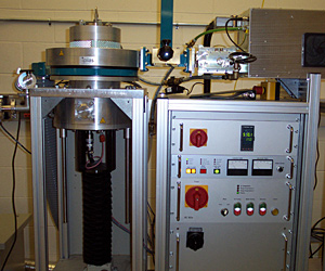
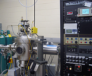
iPLAS MPCVD System

  • 4” plasma source
  • Manual EH tuner
  • Deposition up to 4’’ wafers
  • 6 KW microwave generator (2.45 GHz)
  • Substrate heated up to 800°C
  • Dedicated for growth of nitrogen doped nanocrystalline diamond.

ASTeX MPCVD System

  • 1 KW microwave generator (2.45 GHz)
  • Deposition up to one inch wafer
  • Manual tuning
  • Dedicated to grow boron doped micro/nano diamond coating

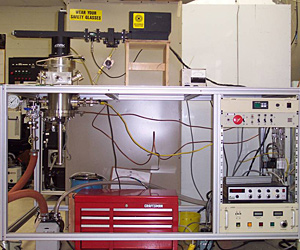
Pulsed Laser Deposition System

  • Substrate heated up to 650°C
  • Multi-target holder system
  • Deposition Chamber can be pumped up to 10-7 Torr

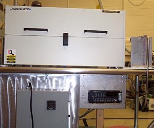
Carbon Nanotube Growth Facility

  • Lindberg Blue Furnace
  • Maximum Temperature 1200°C
  • Programmable Temperature Controller
  • Dedicated for Carbon Nanotube Growth

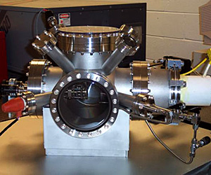
CMS-18 Sputtering System with Load Lock

  • 3 Sputter guns (One RF and two DC power supplies)
  • Substrate holder for up to 6 inch substrates
  • Pneumatic deposition source shutter, switch activated
  • Optional heating and control of substrate
  • Process Gas Inlet/ Pressure Control

Metrology and Characterization Facilities(NMRL)

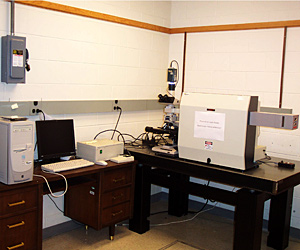
Renishaw MicroRaman Spectroscopy

  • Ar ion laser, 514.5 nm
  • He-Ne laser, 633 nm
  • Semiconductor diode laser, 785 nm
  • -70° Centigrade Peltier cooled CCD detector
  • XYZ motorized mapping stage
  • 100 cm-1 cutoff notch filter
  • Magnification up to 1000x (x5, x20, x50, x100 objectives)
  • Grams 32 spectral analysis software, and geological spectra database
  • 8000 cm-1 extended scanning range
  • 1800 l/mm and 1200 l/mm gratings

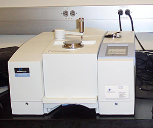
FTIR Spectroscopy

  • Wavelength Range- 7800-350 cm-1
  • Resolution- 0.5 to 64 cm-1
  • Wavelength accuracy- 0.1 to 1600 cm-1
  • Sealed and desiccated optical unit.

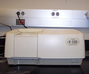
UV-VIS Spectrophotometer

  • Optical system: Double beam, single monochromator with a 1200 grooves/mm concave grating and modified
  • Rowland mount
  • Spectral bandwidth: 2 nm
  • Wavelength range: 190 - 1100 nm
  • Halogen lamp for VIS range (330 - 1100 nm)
  • Wavelength accuracy: ± 0.5 nm
  • Photometric accuracy: ± 0.002 Abs (0 - 0.5 Abs)
  • Detector: Silicon photo-diode (S1337)

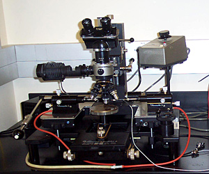
Micro Manipulator 6000 series probe station

  • 4""/100mm Gold-Plated Vacuum Chuck
  • Bausch & Lomb MicroZoom Microscope
  • 2.25x, 8x, 25x Objectives
  • 10x Eyepieces

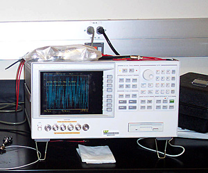
Agilent 4294A Impedance Analyzer

  • Frequency Range 40Hz to 110MHz
  • Dedicated to measure the electrical properties of materials.